There is a category of problem that Wi-Fi cannot solve. A borehole pump on a farm three kilometres from the nearest router. An irrigation valve at the end of a field. A gate motor at a plot entrance. A geyser in a rental unit where you have no access to the tenant's network. In every one of these cases the thing you want to control has mains power available but no data connection, and running a network to it costs more than the control problem is worth.
CellLink32 is my answer to that. It is a 60 × 60 mm six-layer controller board that takes an LTE connection, an ESP32-S3, and a latching relay, and puts them together in a way that is meant to survive being installed once and left alone.
This article walks through the design: what is on the board, why each part was chosen, what the hard problems turned out to be, and what I got wrong the first time. The design is open, so if you want to build on it or argue with it, everything you need to do that is below.
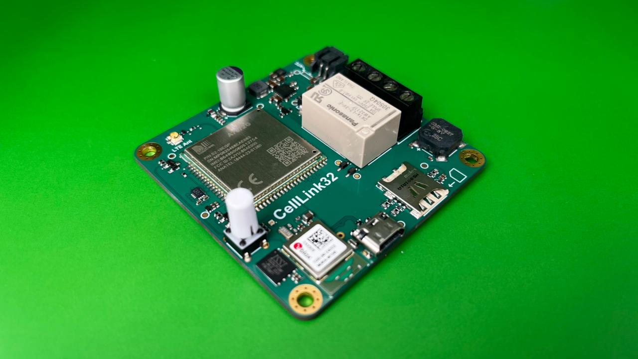
What the board does
At its simplest: a message arrives over the cellular network, and a relay contact closes. A second message opens it again. Everything else on the board exists to make that reliable.
Board Specifications & Key Components
The interesting engineering is not in that list. It is in the interactions between those parts, so let's take them in order.
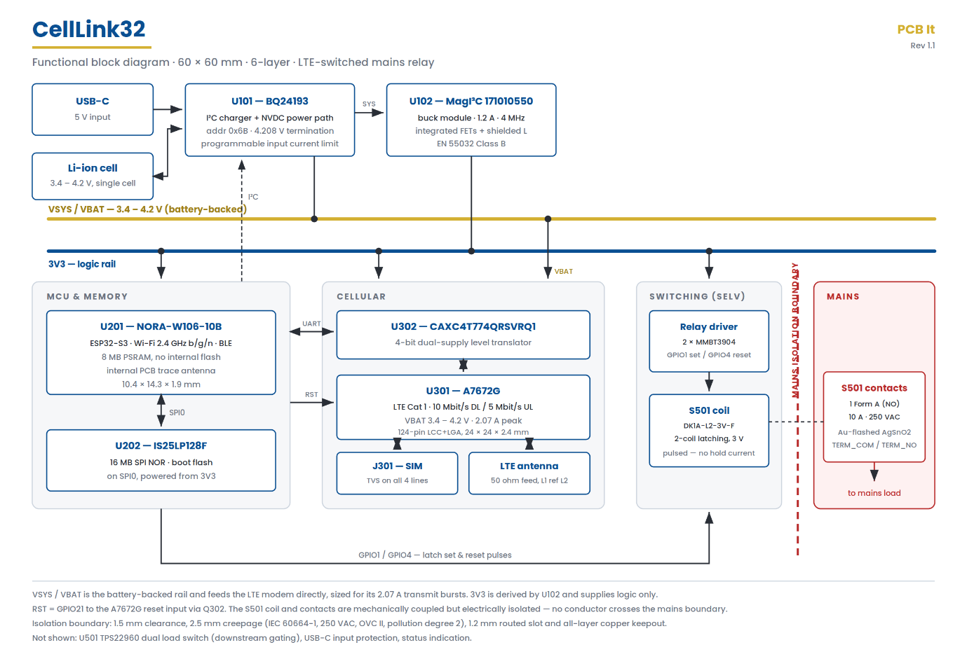
The switching element, and why it latches
The relay is a Panasonic DK1A-L2-3V-F. It is a single-pole normally-open power relay rated 10 A at 250 VAC, with gold-flashed silver tin oxide contacts and a 10 kV surge withstand between coil and contacts. Coil resistance is 45 Ω on a 3 V nominal coil, which works out to roughly 67 mA per pulse.
The word that matters in that part number is the L2. This is a two-coil latching relay. It has a set coil and a reset coil, and it holds its contact position mechanically once you have pulsed one of them. A conventional relay burns coil current continuously for as long as the load is on, which for a board that might be running from a battery during a power interruption is exactly the wrong behaviour. The latching relay draws current only during the transition, measured in milliseconds, and nothing at all in either steady state.
There is a second, less obvious benefit. If the board loses power entirely, a conventional relay drops out and switches your load off. The latching relay does not. A pump that was running before a power cut is still commanded on when power returns, and the board can read its own state and decide what to do rather than having the decision made for it by the power failure.
The cost of latching is that the firmware now has to track state, because the relay will not tell you where it is. That is a fair trade.
What I got wrong: on v1.0 the two coil nets are crossed relative to my intent. GPIO1 closes the contact and GPIO4 opens it, which is the opposite of the labelling in my schematic. It is entirely resolvable in firmware and costs nothing functionally, but it is a good example of a mistake that only surfaces when you put a multimeter on the actual board.
The part that took the longest: mains isolation
This is the section I would encourage anyone building something similar to read twice.
The relay switches mains. That means one corner of the board sits at 230 VAC and the rest of it sits at 3.3 V, and the entire job is making sure those two never meet. Two separate distances govern this:
- Clearance is the shortest path through air between two conductors.
- Creepage is the shortest path along the surface of the insulating material.
Creepage is almost always the binding constraint, because a surface can be contaminated with dust and moisture in a way that open air cannot. Working to IEC 60664-1 for 250 VAC at overvoltage category II and pollution degree 2 on FR4, the figures I designed to between the relay's two contact terminals are 1.5 mm clearance and 2.5 mm creepage. Note that this is functional insulation between two mains nets, not the reinforced insulation you would need at a mains-to-low-voltage barrier, which is a much larger number.
Version 1.0 did not have enough of it. Specifically, the ground plane came closer to the relay's switch contacts than I was comfortable with.
Two things fix this in v1.1.
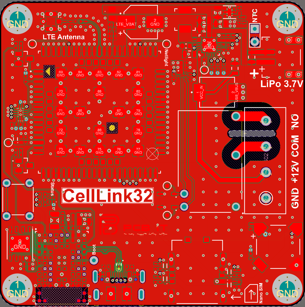
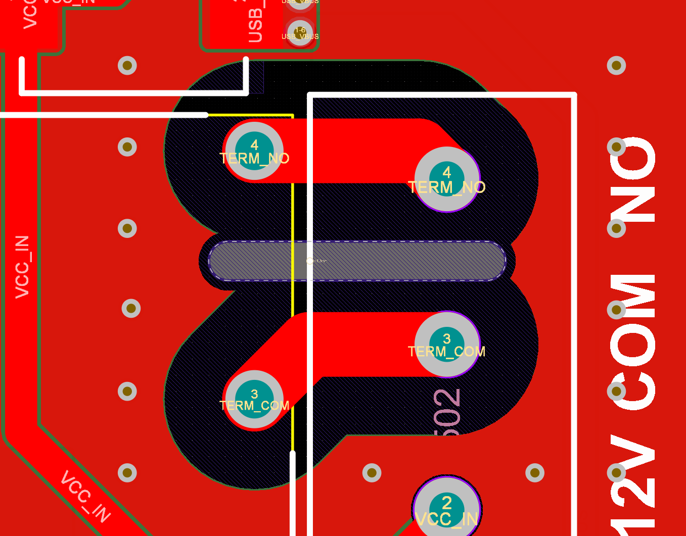
A routed slot. Cutting a slot in the board between the two mains terminals converts a short surface path into a long one that has to travel down one wall of the slot, across the bottom, and up the other side. The slot has to be at least 1.0 mm wide, and I am using 1.2 mm. This is not an arbitrary number: IEC 60664-1 treats any groove narrower than 1 mm at pollution degree 2 as if it were bridged with contamination, which means a 0.8 mm slot buys you exactly no creepage credit while still costing you a routing operation. It also happens to sit comfortably above JLCPCB's minimum routed slot width. The wrap-around at each end of the slot needs checking too, because a slot that does not extend far enough simply moves the shortest path around its ends.
All-layer copper keep-outs. This is the one that catches people. Altium's clearance rules are two-dimensional and per-layer. They will happily tell you a mains track has adequate clearance on the top layer while an inner ground plane floods solid copper directly beneath it, one prepreg layer away. The clearance rule cannot see this because it is not looking in that direction. The only reliable answer is an explicit keep-out that spans every layer, plus the physical slot.
A note on DRC violations that are not violations
Once the slot is in, Altium generates clearance violations between the two mains nets that are not real. The checker sees copper 1.5 mm apart on the same layer and flags it against my global 2 mm AC Power net class rule. It cannot account for the slot, because a 2D check has no concept of the board material being absent.
The wrong fix is to relax the global rule, because that rule is what guards the far more important mains-to-low-voltage boundary. The right fix is a scoped, higher-priority rule set to 1.5 mm between those two specific nets. The general rule keeps doing its job everywhere else, and the false positives disappear without anything being weakened.
One related habit worth adopting: define your safety-critical net classes at schematic level, not in the PCB. Net classes created in the PCB editor can have their membership cleared by an ECO sync when you next import changes from the schematic. Losing the AC_Power class membership silently means losing every clearance rule scoped to it, on the one part of the board where you cannot afford that.
The cellular side
The modem is a SIMCom A7672G, an LTE Cat 1 module in a 24 × 24 × 2.4 mm package with 124 pins, 80 LCC in the outer ring and 44 LGA inside. Cat 1 gives 10 Mbit/s down and 5 Mbit/s up, which is enormous overkill for sending the word "on" but is the sensible category for a device that also needs to work on networks that are winding down their 2G and 3G services.
The specification that shapes the whole power design is on page 20 of SIMCom's hardware design document: VBAT is 3.4 V to 4.2 V, and peak current reaches 2.07 A. Not average. Peak, during transmit bursts. SIMCom asks for the supply to hold its droop under 300 mV at that current, and recommends at least 300 µF of bulk capacitance nearby.
That single line is why this board has a battery rather than just a USB input. A single-cell Li-ion sits naturally in the 3.4–4.2 V window the modem wants, has effectively zero source impedance at 2 A compared with a USB cable and connector, and rides through the transmit bursts without the rest of the board browning out. The modem is powered from the battery-backed rail directly, not from the 3.3 V logic rail.
The SIM socket is on the same sheet, with TVS protection on all four signal lines. Worth knowing if you are working with this modem: the A7672G does not re-initialise the SIM on hot insertion. It will emit a +CPIN: SIM REMOVED unsolicited result code when you pull the card, but putting a card back in does not bring the interface up again without a reset. Design your enclosure so nobody expects to hot-swap.
Between the modem and the MCU sits a TI CAXC4T774QRSVRQ1 four-bit dual-supply bus transceiver, handling the level translation between the modem's IO voltage and the MCU's 3.3 V. Channel directions verified individually on the bench, because getting one backwards on a translator is a silent failure that looks like a dead UART.
It works!
The satisfying part of bring-up. The board registers on Vodacom (MCC-MNC 655-01), EUTRAN Band 41, at −90 dBm RSRP, on the bench in Pretoria with the on-board antenna.
[IMAGE 4 — terminal capture] Screenshot of the AT+CPSI? response showing the network registration, band, and signal level. Concrete evidence beats a claim.
If you are tuning an LTE antenna yourself, use RSRP rather than plain RSSI. RSSI includes interference and neighbouring-cell energy, so it will move around in ways that have nothing to do with your antenna. RSRP is a per-resource-element measurement of your serving cell and is a far cleaner signal to optimise against. Read it with AT+CESQ or AT+CPSI?, lock the band with AT+CNBP so you are comparing like with like, and average 30 to 60 samples per configuration. Antennas are noisy things to measure and single readings will lie to you.
The brain
The MCU is a u-blox NORA-W106-10B: an ESP32-S3 wireless module, 10.4 × 14.3 × 1.9 mm, with Wi-Fi b/g/n on 2.4 GHz and Bluetooth LE. The Wi-Fi and BLE antenna is an internal PCB trace antenna inside the module itself, licensed from Abracon, with the RF signal not brought out to any pin. That is a genuine convenience: the only antenna I have to design on this board is the LTE one.
Choosing the -10B variant specifically has one consequence that is easy to miss. That variant swap the 8 MB of embedded flash for 8 MB of embedded PSRAM. It has no internal flash at all, so external flash is mandatory for code storage. That is the IS25LP128F, 16 MB, confirmed on the bench with esptool reading back manufacturer ID 0x9D.
Two things about connecting it that cost me time:
- Use SPI0, not FSPI. The ESP32-S3 will only boot from flash on the SPI0 bus. FSPI is a general-purpose peripheral and code placed on it is not bootable. On this module the FSPI pins are unusable anyway, because the internal octal-SPI PSRAM occupies them.
- Power the flash from 3.3 V, not VDD_SPI. The VDD_SPI rail defaults to 1.8 V on the ESP32-S3, and the IS25LP128F needs 2.6 V minimum. Wiring the flash to VDD_SPI gives you a part that is technically connected and completely non-functional. On the modules I received, the VDD_SPI eFuse was already factory-burned to 3.3 V, which means GPIO45 (the strapping pin that would otherwise select it) is irrelevant here. I still ran the flash from the 3.3 V rail directly, because relying on an eFuse state you did not burn yourself is not a thing to build a product on.
A related first-boot surprise: a blank factory flash produces a bootloop with invalid header: 0xffffffff on the serial console. This is normal and resolves itself on the first successful upload. I lost an evening to it convinced I had a hardware fault.
Power architecture
The chain runs USB-C → BQ24193 → battery and system rail → MagI³C buck → 3.3 V.
The BQ24193 is TI's I²C-controlled single-cell charger with narrow-VDC power-path management. It integrates the reverse-blocking FET, both switching FETs, and the BATFET, and it does something a simple charger does not: the power path lets the system draw current from the input and the battery simultaneously, sharing between them as needed. When the modem asks for its 2 A burst and the USB input cannot supply it, the battery makes up the difference automatically, and the input stays inside its current limit rather than collapsing. Dynamic power management confirmed active on the bench.
It lives at I²C address 0x6B. Charge termination voltage reads back as 4.208 V, which sits fractionally above the 4.2 V I had set as a design ceiling. This is a known and accepted deviation, not an oversight. Input current limit is set by a resistor on the ILIM pin, and that value is being revised upward in v1.1 to give the modem more headroom on a wall adapter.
The 3.3 V rail comes from a Würth MagI³C 171010550. This is a fully integrated buck module in a 2.5 × 2.5 mm LGA-6EP package with the controller, both MOSFETs and a shielded inductor inside: 2.5–5.5 V in, adjustable 0.8–5.5 V out, 1.2 A, switching at a fixed 4 MHz. Two reasons for a module rather than a discrete regulator on this board. The obvious one is area, on a board that is already tight. The less obvious one is that Würth characterise it as compliant with EN 55032 Class B radiated emissions, and on a board with an LTE transmitter and a 2.4 GHz radio, starting from a switcher with known and shielded emissions behaviour removes an entire category of problem before it exists.
A TPS22960 dual load switch handles selective power gating downstream.
The stack-up
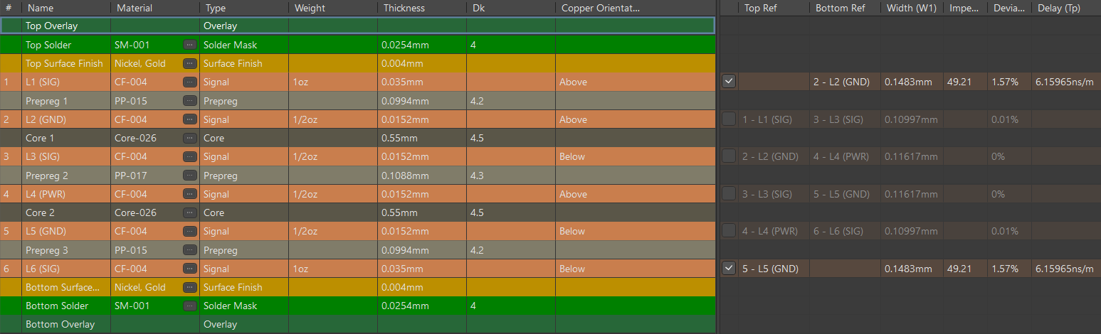
Six layers, JLC06161H-3313, ENIG finish, TG155 substrate.
Six layers on a 60 × 60 mm board with this component count is arguably more than the routing density demands. It is not there for routing. It is there so that the RF trace to the LTE antenna has an uninterrupted reference plane immediately beneath it, and so that the mains section can have genuinely solid, controlled copper boundaries rather than a compromise between routing and isolation.
The LTE antenna feed is a 0.148 mm (5.83 mil) trace on L1 referenced to L2 through PP-015 prepreg, with Er = 4.2 and a dielectric height of 3.91 mil. That geometry calculates to approximately 49.7 Ω, which is as close to 50 Ω as the available stack-up permits.
I want to be straight about the limits of that number. It is a calculation from nominal stack-up parameters. Actual permittivity varies with frequency, resin content and manufacturing tolerance, and the calculation says nothing at all about the antenna's match at the far end of the trace. Confirming real-world VSWR at Band 41, around 2.6 GHz, requires a vector network analyser against the physical board. That measurement is still outstanding and I am not going to pretend a field solver result is the same thing.
A few smaller layout decisions worth passing on:
- Mounting hole vias use direct connect, not thermal relief. A thermal relief antipad can strand a via outside the copper pour entirely, leaving it connected to nothing. Thermal relief is right for signal-return ground pins on ICs; it is wrong for mounting pads, exposed thermal pads on power devices, and high-current returns.
- The 32.768 kHz crystal (a CM315D32768DZFT) uses 18 pF load capacitors, which is correct given roughly 5 pF internal and 2 pF of stray capacitance. The crystal is rotated 90° so its pins align vertically with the module's stacked XTAL pads.
- Ground stitching vias on the SIM lines are unnecessary. SIM signalling runs at 1–5 MHz. Via-proximity stitching rules exist for fast edges, and applying them here just costs board area and drill count. I had over-specified this initially.
Designing for the assembler
One practical note for anyone taking a design like this to a turnkey assembler. JLCPCB does not stock the A7672G-LABE, but does stock the A7670G-LABE (part C22462360), which is a drop-in in the same 124-pin 24 × 24 × 2.4 mm package with an identical band set for the LABE suffix.
Two things to check before committing to that swap:
- There is an MSL discrepancy in the listings. JLCPCB shows the part as moisture sensitivity level 1; SIMCom rates it MSL 3. Those are meaningfully different handling requirements, and it is worth raising with the assembler before a reel is committed rather than after.
- The GNSS and Bluetooth functions are suffix features of the F-prefix variants, not the L-prefix ones. On a LABE part, eight pins associated with those functions (90, 93, 95–98, 100 and 116) should be left genuinely floating: no net, no polygon, no stitching. Leaving them truly unconnected keeps the footprint tolerant of a future F-suffix variant should GNSS ever be wanted, at zero cost today.
The module also requires standard PCBA rather than the economic service, and an assembly fixture.
What is still open
Being honest about the unfinished parts is more useful than pretending there aren't any.
- LTE antenna VSWR at Band 41 is unmeasured. Needs a VNA against the physical board. The 49.7 Ω trace impedance is a calculation, not a measurement.
- The input current limit resistor is changing in v1.1, and the full power budget is not closed until the charger's ILIM constant is confirmed from the electrical characteristics table rather than from the applications section.
- Slot creepage wrap-around at both ends of the routed slot needs a final check against the 2.5 mm target.
- The card-detect wiring constraint on the SIM socket is behaving in a way I have not yet explained to my own satisfaction. It works. I do not fully know why it works.
What I would tell someone starting this
Three things, none of which are about this board specifically.
- Measure it, do not assume it. Almost everything in this article that surprised me was found with a multimeter, a logic analyser or a serial console, not by reading a datasheet more carefully. The crossed relay coils, the eFuse state, the flash manufacturer ID: all of these were things I believed I already knew.
- The design rule checker is a tool, not an authority. It found nothing wrong with the inner-layer copper under my mains tracks, because that is not a question it is capable of asking. It flagged a dozen violations at the slot that were not real. Understanding where a checker's model stops matching physical reality is most of the skill in using one.
- Get the safety boundary right before anything else is pretty. Layout aesthetics matter to me and I will spend time on them. But the clearances, the creepage, the keep-outs and the slot are the part of this board that could hurt somebody, and they are the part that got settled first and revisited most.
CellLink32 is designed by PCB It. If you have a prototype that needs to become a manufacturable product, that is what I do.